- 您现在的位置:买卖IC网 > Sheet目录3871 > PIC16F72-I/ML (Microchip Technology)IC PIC MCU FLASH 2KX14 28-QFN
119
2535J–AVR–08/10
ATtiny13
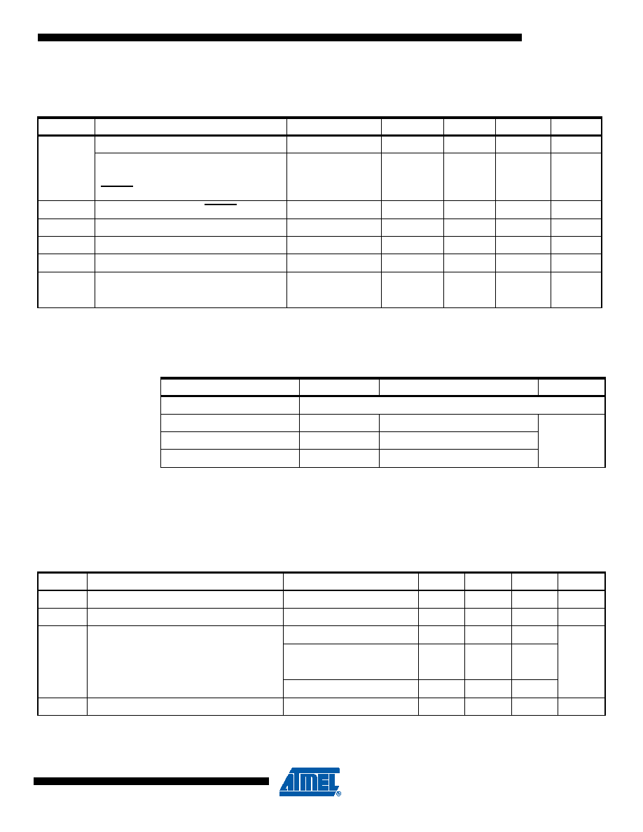
18.5 System and Reset Characteristics
Note:
1. The Power-on Reset will not work unless the supply voltage has been below VPOT (falling)
18.5.1
Brown-Out Detection
Note:
1. VBOT may be below nominal minimum operating voltage for some devices. For devices where
this is the case, the device is tested down to VCC = VBOT during the production test. This guar-
antees that a Brown-out Reset will occur before VCC drops to a voltage where correct
operation of the microcontroller is no longer guaranteed.
18.6 Analog Comparator Characteristics
Note:
All parameters are based on simulation results and they are not tested in production
Table 18-4.
Reset, Brown-out and Internal Voltage Reference Characteristics
Symbol
Parameter
Condition
Min
Typ
Max
Units
VPOT
Power-on Reset Threshold Voltage (rising)
TA = -40 to +85°C1.2
V
Power-on Reset Threshold Voltage
(falling)(1)
TA = -40 to +85°C1.1
V
VRST
RESET Pin Threshold Voltage
VCC = 1.8V - 5.5V
0.2 VCC
0.9 VCC
V
tRST
Minimum pulse width on RESET Pin
VCC = 1.8V - 5.5V
2.5
s
VHYST
Brown-out Detector Hysteresis
50
mV
tBOD
Min Pulse Width on Brown-out Reset
2
s
VBG
Bandgap reference voltage
1.0
1.1
1.2
V
tBG
Bandgap reference start-up time
40
70
s
IBG
Bandgap reference current consumption
15
s
Table 18-5.
VBOT vs. BODLEVEL Fuse Coding
BODLEVEL [1:0] Fuses
Min(1)
Typ(1)
Max(1)
Units
11
BOD Disabled
10
1.8
V
01
2.7
00
4.3
Table 18-6.
Analog Comparator Characteristics, TA = -40°C to +85°C
Symbol
Parameter
Condition
Min
Typ
Max
Units
VAIO
Input Offset Voltage
VCC = 5V, VIN = VCC / 2
< 10
40
mV
ILAC
Input Leakage Current
VCC = 5V, VIN = VCC / 2
-50
50
nA
tAPD
Analog Propagation Delay
(from saturation to slight overdrive)
VCC = 2.7V
750
ns
VCC = 4.0V
500
Analog Propagation Delay
(large step change)
VCC = 2.7V
100
VCC = 4.0V
75
tDPD
Digital Propagation Delay
VCC = 1.8V - 5.5
1
2
CLK
发布紧急采购,3分钟左右您将得到回复。
相关PDF资料
XF2R34154A
CONN FPC 34POS 0.5MM PITCH SMD
XF2R24154A
CONN FPC 24POS 0.5MM PITCH SMD
PIC18F45K20-I/ML
IC PIC MCU FLASH 16KX16 44QFN
PIC18F14K50-I/SO
IC PIC MCU FLASH 8KX16 20-SOIC
PIC16F628A-I/SS
IC MCU FLASH 2KX14 EEPROM 20SSOP
PIC18LF43K22-I/PT
IC PIC MCU 8KB FLASH 44TQFP
DSPIC33FJ16MC101-I/SO
IC DSP 16BIT 16KB 20SOIC
PIC12C672-04I/SM
IC MCU OTP 2KX14 A/D 8-SOIJ
相关代理商/技术参数
PIC16F72-I/MLG
功能描述:8位微控制器 -MCU 3.5KB 128 RAM 22 I/O Lead Free Package RoHS:否 制造商:Silicon Labs 核心:8051 处理器系列:C8051F39x 数据总线宽度:8 bit 最大时钟频率:50 MHz 程序存储器大小:16 KB 数据 RAM 大小:1 KB 片上 ADC:Yes 工作电源电压:1.8 V to 3.6 V 工作温度范围:- 40 C to + 105 C 封装 / 箱体:QFN-20 安装风格:SMD/SMT
PIC16F72-I/SO
功能描述:8位微控制器 -MCU 3.5KB 128 RAM 22 I/O
RoHS:否 制造商:Silicon Labs 核心:8051 处理器系列:C8051F39x 数据总线宽度:8 bit 最大时钟频率:50 MHz 程序存储器大小:16 KB 数据 RAM 大小:1 KB 片上 ADC:Yes 工作电源电压:1.8 V to 3.6 V 工作温度范围:- 40 C to + 105 C 封装 / 箱体:QFN-20 安装风格:SMD/SMT
PIC16F72-I/SO
制造商:Microchip Technology Inc 功能描述:8BIT FLASH MCU SMD 16F72 SOIC28
PIC16F72-I/SOG
功能描述:8位微控制器 -MCU 3.5KB 128 RAM 22 I/O Lead Free Package RoHS:否 制造商:Silicon Labs 核心:8051 处理器系列:C8051F39x 数据总线宽度:8 bit 最大时钟频率:50 MHz 程序存储器大小:16 KB 数据 RAM 大小:1 KB 片上 ADC:Yes 工作电源电压:1.8 V to 3.6 V 工作温度范围:- 40 C to + 105 C 封装 / 箱体:QFN-20 安装风格:SMD/SMT
PIC16F72-I/SP
功能描述:8位微控制器 -MCU 3.5KB 128 RAM 22 I/O
RoHS:否 制造商:Silicon Labs 核心:8051 处理器系列:C8051F39x 数据总线宽度:8 bit 最大时钟频率:50 MHz 程序存储器大小:16 KB 数据 RAM 大小:1 KB 片上 ADC:Yes 工作电源电压:1.8 V to 3.6 V 工作温度范围:- 40 C to + 105 C 封装 / 箱体:QFN-20 安装风格:SMD/SMT
PIC16F72-I/SP
制造商:Microchip Technology Inc 功能描述:IC 8BIT FLASH MCU 16F72 SDIL28
PIC16F72-I/SS
功能描述:8位微控制器 -MCU 3.5KB 128 RAM 22 I/O
RoHS:否 制造商:Silicon Labs 核心:8051 处理器系列:C8051F39x 数据总线宽度:8 bit 最大时钟频率:50 MHz 程序存储器大小:16 KB 数据 RAM 大小:1 KB 片上 ADC:Yes 工作电源电压:1.8 V to 3.6 V 工作温度范围:- 40 C to + 105 C 封装 / 箱体:QFN-20 安装风格:SMD/SMT
PIC16F72-I/SS
制造商:Microchip Technology Inc 功能描述:8BIT FLASH MCU SMD 16F72 SSOP28